Loading...
Searching...
No Matches
Technical Data
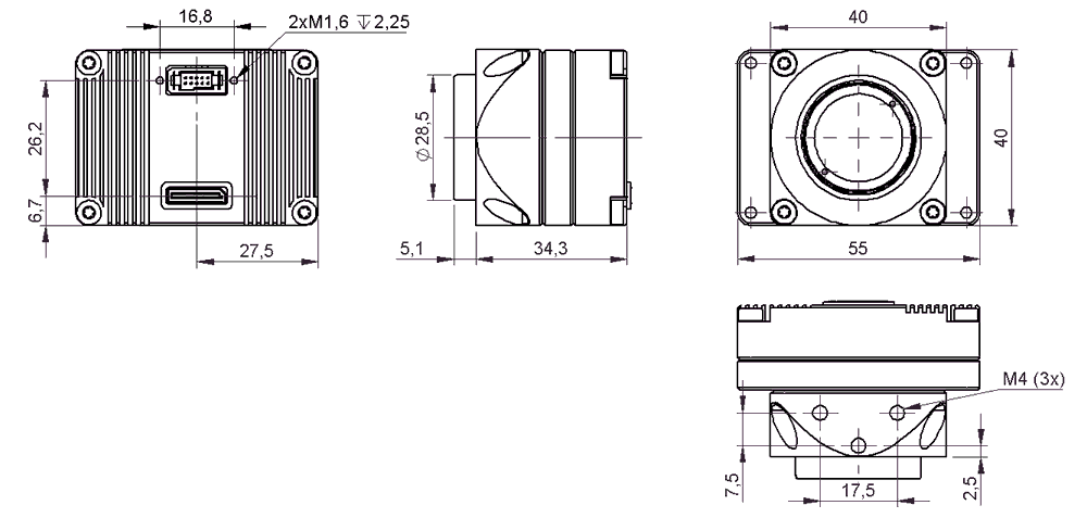
BVS CA-BN2
Dimensions
BVS CA-BN2-xxxxx-x5x110 (Standard housing with N4e interface)
| BVS CA-BN2 | |
| Size of body (w x h x l) | 40 x 40 x 27 mm |
BVS CA-BN2-xxxxx-x00010 (Board-level with N4e interface)
| BVS CA-BN | |
| Size of body (w x h x l) | 37 x 37 x 6.9 mm |
BVS CA-BN2-xxxxx-x5x1H0 (Standard housing with OCuLink)
| BVS CA-BN2 | |
| Size of body (w x h x l) | 40 x 40 x 34.3 mm |
BVS CA-BN4
Dimensions
BVS CA-BN4-xxxxx-x5x510 (Board-level with N4e interface)
| BVS CA-BN4 | |
| Size of body (w x h x l) | 55 x 40 x 22.1 mm |
BVS CA-BN4-xxxxx-x5x1H0 (Standard housing with OCuLink)
| BVS CA-BN4 | |
| Size of body (w x h x l) | 55 x 40 x 34.3 mm |
N4e Interface
The N4e interface provides PCIe Gen.2 and various I/O functionality on a single 70-pin Board-to-Board connector. The main features of the user I/O interface are
- 4 digital inputs,
- 4 digital outputs,
- a UART interface for serial communication, and
- a I2C two wire serial interface.
"Camera connector"
- Hirose DF40GB(3.0)-70DS-0.4V
"Mating Connector"
Used for accessory IO Boards or customer implementation.
- Hirose DF40GB-70DP-0.4V
"Mechanical characteristics"
- 70-pin, 0.4mm pitch, shielded, stacking height: 3.0mm
- Steel spacers (height 3mm). Screws M1.6, max. screw depth 1.8mm.
Pin assignment
- Note
- The red dot marks pin 1 of Hirose DF40GB(3.0)-70DS-0.4V.
| Pin | Signal | Description |
| 1 | VCC_IN | Input Voltage (5V-12V) |
| 2 | VCC3V3 | Power Output, max. 10mA for customer use |
| 3 | VCC_IN | Input Voltage (5V-12V) |
| 4 | I2C_SCL_USER | I2C_USER (see details below) LVCMOS 3.3V IO level |
| 5 | VCC_IN | Input Voltage (5V-12V) |
| 6 | I2C_SDA_USER | I2C_USER (see details below) LVCMOS 3.3V IO level |
| 7 | DigIn0 | Digital input (with level shifter) Voltage reference VCC_IO |
| 8 | UART_RX | LVCMOS 3.3V IO level 100 Ohm series resistor placed on mainboard |
| 9 | DigIn1 | Digital input (with level shifter) Voltage reference VCC_IO |
| 10 | UART_TX | LVCMOS 3.3V IO level 100 Ohm series resistor placed on mainboard |
| 11 | GND | Ground |
| 12 | GND | Ground |
| 13 | GND | Ground |
| 14 | GND | Ground |
| 15 | PCIe_CLK_P | PCIE_CLK + (differential) |
| 16 | x | Do not connect, internal use |
| 17 | PCIe_CLK_N | PCIE_CLK - (differential) |
| 18 | x | Do not connect, internal use |
| 19 | GND | Ground |
| 20 | GND | Ground |
| 21 | PCIe_TX0_P | PCIe Transmitter (differential) |
| 22 | x | Do not connect, internal use |
| 23 | PCIe_TX0_N | PCIe Transmitter (differential) |
| 24 | x | Do not connect, internal use |
| 25 | GND | Ground |
| 26 | GND | Ground |
| 27 | GND | Ground |
| 28 | GND | Ground |
| 29 | DigIn2 | Digital input (with level shifter) Voltage reference VCC_IO |
| 30 | GND | Ground |
| 31 | DigIn3 | Digital input (with level shifter) Voltage reference VCC_IO |
| 32 | PCIe_RX3_P | PCIe Receiver (differential) |
| 33 | GND | Ground |
| 34 | PCIe_RX3_N | PCIe Receiver (differential) |
| 35 | PCIe_TX1_P | PCIe Transmitter (differential) |
| 36 | GND | Ground |
| 37 | PCIe_TX1_N | PCIe Transmitter (differential) |
| 38 | PCIe_RX0_P | PCIe Receiver (differential) |
| 39 | GND | Ground |
| 40 | PCIe_RX0_N | PCIe Receiver (differential) |
| 41 | PCIe_PERST_N | Reset |
| 42 | GND | Ground |
| 43 | GND | Ground |
| 44 | GND | Ground |
| 45 | GND | Ground |
| 46 | GND | Ground |
| 47 | PCIe_TX2_P | PCIe Transmitter (differential) |
| 48 | PCIe_RX2_P | PCIe Receiver (differential) |
| 49 | PCIe_TX2_N | PCIe Transmitter (differential) |
| 50 | PCIe_RX2_N | PCIe Receiver (differential) |
| 51 | GND | Ground |
| 52 | GND | Ground |
| 53 | PCIe_TX3_P | PCIe Transmitter (differential) |
| 54 | PCIe_RX1_P | PCIe Receiver (differential) |
| 55 | PCIe_TX3_N | PCIe Transmitter (differential) |
| 56 | PCIe_RX1_N | PCIe Receiver (differential) |
| 57 | GND | Ground |
| 58 | GND | Ground |
| 59 | GND | Ground |
| 60 | GND | Ground |
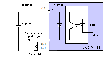
| 61 | DigOut0 | Digital output (with level shifter) Voltage reference VCC_IO |
| 62 | x | Do not connect, internal use |
| 63 | DigOut1 | Digital output (with level shifter) Voltage reference VCC_IO |
| 64 | x | Do not connect, internal use |
| 65 | DigOut2 | Digital output (with level shifter) Voltage reference VCC_IO |
| 66 | VCC_IN | Input Voltage (5V-12V) |
| 67 | DigOut3 | Digital output (with level shifter) Voltage reference VCC_IO |
| 68 | VCC_IN | Input Voltage (5V-12V) |
| 69 | VCC_IO | Voltage reference for digital inputs / outputs. |
| 70 | VCC_IN | Input Voltage (5V-12V) |
- Note
- Additional shield pins are connected to GND.
Electrical characteristics of signals
Input Voltage
| Parameter | Description | min | nom | max | Unit |
| VCC_IN | 5 | 12 | 17 | V | |
| IVCC_IN | 1.8 | A | |||
| I per pin | 0.3 | A |
VCC_IO / DIGIN / DIGOUT
| Parameter | Description | min | nom | max | Unit |
| VCC_IO | I/O voltage power | 1.8 | 3.3 | 5.5 | V |
| UDIG_IN_LOW | Low-level input voltage | 0.8 | V | ||
| UDIG_IN_HIGH | High-level input voltage | 0.7 x VCC_IO | V | ||
| IOH | Output current for VCC_IO = 3.3 V | -24 | mA | ||
| IOL | Output current for VCC_IO = 3.3 V | 24 | mA | ||
| UDIG_OUT_HIGH | Output voltage for VCC_IO = 3.3 V, IOUT= -24 mA | 2.4 | V | ||
| UDIG_OUT_LOW | Output voltage for VCC_IO = 3.3 V, IOUT= 24 mA | 0.55 | V |
- Note
- Digital I/Os include Level Shifters which allow customized I/O levels. Output characteristics given for VCC_IO = 3.3 V. For other values see datasheet SN74LVC2T45
Serial Interface, I2C and Power Down
| Signal | Parameters / Properties | min | nom | max | Unit |
| PCIe_PERST_N | Reset | 3.3 | |||
| PCIe_PERST_N Input Low Voltage | -0.5 | 0.8 | V | ||
| PCIe_PERST_N Input High Voltage | 2 | 3.8 | V | ||
| UART_RX / UART_TX | Voltage level | 3.3 | 3.4 | V | |
| The camera provides a UART Interface for serial communication (internally protected by 100Ohm series resistor) | |||||
| I2C_SCL / I2C_SDA | USER_I2C for customer applications | 3.3 | V |
Add-in cards for the BVS CA-BN for Embedded (N4e) Interface
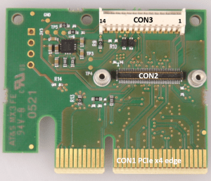
BNE-IF-PCIeX4-N4e-IO14
Add-in card for connecting the camera to the PCIe x4 slot of a host board. The board includes
- the N4e interface (CON2)
- a 14-pin I/O connector (CON3) and
- the PCIe x4 edge (CON1).
The add-in card is compliant with PCIe 2.0 mainboard or higher (up to 1600 MB/s). Dimensions: 37.5 mm x 46 mm.
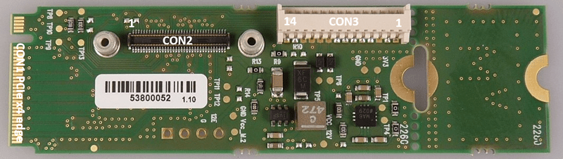
BNE-IF-M2M-N4e-IO14
M.2-M-Key add-in card for connecting the camera to the PCIe x4 slot of a host board. The board includes
- the N4e interface (CON2)
- a 14-pin I/O connector (CON3) and
- the PCIe x4 edge (CON1).
The add-in card is compliant with PCIe 2.0 mainboard or higher (up to 1600 MB/s). Dimensions: 22 mm x 80 mm (or 60 mm).
Pin assignments
14-pin I/O connector (CON3)
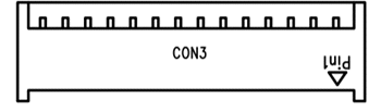
- Part type:
- Wire-to-Board connector 1.25 mm Molex PicoBlade 53048_1410
- Connecting part:
- Molex 0510211400, 1.25 mm Wire-to-Board connection receptacle crimp housing, applicable terminal 50058-8000, 50079-8000 series
| Pin | I/O | Signal | Description |
| 1 | Out | DigOut0 | Digital Output |
| 2 | Out | DigOut1 | Digital Output |
| 3 | Out | DigOut2 | Digital Output |
| 4 | Out | DigOut3 | Digital Output |
| 5 | In | DigIn0 | Digital Input |
| 6 | In | DigIn1 | Digital Input |
| 7 | In | DigIn2 | Digital Input |
| 8 | In | DigIn3 | Digital Input |
| 9 | Out | RS232_TXD | Serial Interface RS232_TXD |
| 10 | In | RS232_RXD | Serial Interface RS232_RXD |
| 11 | GND | GND | Ground |
| 12 | POWER | VCC_IO | Not connected |
| 13 | Out | I2C_SCL_USER | I2C Clock |
| 14 | BI | I2C_SDA_USER | I2C Data |
"Electrical characteristics of signals"
"VCC_IO / DIGIN / DIGOUT"
| Parameter | Description | min | nom | max | Unit |
| VCC_IO | I/O voltage power (connected to 3.3 V on-board) | 3.3 | V | ||
| UDIG_IN_LOW | Low-level input voltage | 0 | 0.8 | V | |
| UDIG_IN_HIGH | High-level input voltage | 2 | 3.5 | V | |
| IOH | High-level output current | -10 | mA | ||
| IOL | Low-level output current | 10 | mA | ||
| UDIG_OUT_HIGH | High-level output voltage | 2.4 | 3.3 | V | |
| UDIG_OUT_LOW | High-level output voltage | 0.0 | 0.55 | V |
"Serial interface RS232"
| Parameter | Description | min | nom | max | Unit |
| EIA/TIA-232E Input Voltage Range* | -30 | +30 | V | ||
| EIA/TIA-232E Input Threshold Low | 0.6 | 1.3 | V | ||
| EIA/TIA-232E Input Threshold High | 1.6 | 2.4 | V | ||
| EIA/TIA-232E Input Hysteresis | 0.4 | mA | |||
| EIA/TIA-232E Input Resistance | 3 | 5 | 7 | V | |
| Output Voltage Swing | ±5.0 | ±5.7 | V | ||
| RS-232 Output Short-Circuit Current | ±15 | mA | |||
| ESD PROTECTION | Human body model air discharge Human body model contact discharge | ±15 ±8 | kV kV | ||
| TIMING CHARACTERISTICS | Maximum Data Rate | 115 | kbps |
"I2C_USER"
| Signal | Parameter | min | nom | max | Unit |
| UI2C - I2C_SCL_USER / I2C_SDA_USER | 3.3 | V | |||
| U_IN_LOW | VIL (low level input voltage) | 0 | 0.15 | V | |
| U_IN_HIGH | VIH (high level input voltage) | 2.9 | 3.3 | V | |
| U_OUT_HIGH | depending on user pullup (default 2k) | 2.2 | V | ||
| U_OUT_LOW | Digital output (IOUT=1mA) | 0.4 | V | ||
| Frequency | Interface clock rate | 100 | 400 | kHz |
- Note
- 10K pull up resistor to 3.3 V is intergrated. For 400 kHz operation additional 2K pull up is recommended.
OCuLink
The OCuLink interface provides PCIe Gen.2 functionality on a single 42-pin connector.
"Camera connector"
- Amphenol type G14A42211912HRV
"Matching cable"
Used for accessory IO Boards or customer implementation.
- OCuLink standard cable, for example Molex 2060611151/2021431003 or similar from other suppliers
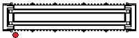
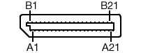
Pin assignment
- Note
- The red dot marks pin 1.
| Pin | Signal | Description |
| A1 | - | Do not connect |
| A2 | GND | Ground |
| A3 | PCIe_RX0_P | PCIe Receiver IN (differential) |
| A4 | PCIe_RX0_N | PCIe Receiver IN (differential) |
| A5 | GND | Ground |
| A6 | PCIe_RX1_P | PCIe Receiver IN (differential) |
| A7 | PCIe_RX1_N | PCIe Receiver IN (differential) |
| A8 | GND | Ground |
| A9 | - | Do not connect |
| A10 | WAKE_PCIE | IN CWAKE |
| A11 | GND | Ground |
| A12 | PCIe_CLK_P | IN PCIE_CLK + |
| A13 | PCIe_CLK_N | IN PCIE_CLK + |
| A14 | GND | Ground |
| A15 | PCIe_RX2_P | PCIe Receiver IN (differential) |
| A16 | PCIe_RX2_N | PCIe Receiver IN (differential) |
| A17 | GND | Ground |
| A18 | PCIe_RX3_P | PCIe Receiver IN (differential) |
| A19 | PCIe_RX3_N | PCIe Receiver IN (differential) |
| A20 | GND | Ground |
| A21 | PWR_IN | Power-In |
| B1 | PWR_IN | Power-In |
| B2 | GND | Ground |
| B3 | PCIe_TX0_P | PCIe Transmitter OUT (differential) |
| B4 | PCIe_TX0_N | PCIe Transmitter OUT (differential) |
| B5 | GND | Ground |
| B6 | PCIe_TX1_P | PCIe Transmitter OUT (differential) |
| B7 | PCIe_TX1_N | PCIe Transmitter OUT (differential) |
| B8 | GND | Ground |
| B9 | - | Do not connect |
| B10 | - | Do not connect |
| B11 | GND | Ground |
| B12 | PCIe_PERST_N | IN Reset |
| B13 | CPRSNT | IN PRESENT |
| B14 | GND | Ground |
| B15 | PCIe_TX2_P | PCIe Transmitter OUT (differential) |
| B16 | PCIe_TX2_N | PCIe Transmitter OUT (differential) |
| B17 | GND | Ground |
| B18 | PCIe_TX3_P | PCIe Transmitter OUT (differential) |
| B19 | PCIe_TX3_N | PCIe Transmitter OUT (differential) |
| B20 | GND | Ground |
| B21 | - | Do not connect |
Directions of the PCIe signals (Transmitter/Receiver) are from the FPGA to the add-in card.
Electrical characteristics of signals
Input Voltage
| Signal | min | nom | max | Unit |
| V_IN | - | 5 | - | V |
| IVCC_IN | 2 | A | ||
| I per pin | 0.5 | A |
Power Down
| Signal | Properties | min | nom | max | Unit |
| PCIe_PERST_N | Voltage level | - | 3.3 | - | V |
| VIL (low level input voltage) | -0.5 | - | 0.8 | V | |
| VIH (high level input voltage) | 2 | - | 3.8 | V | |
| WAKE_PCIe | Voltage level | - | 3.3 | - | V |
| VIL (low level input voltage) | -0.5 | - | 0.8 | V | |
| VIH (high level input voltage) | 1 | - | 3.8 | V | |
| Current WAKE_PCIe | - | - | 4 | mA |
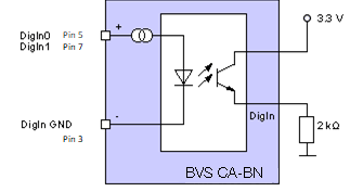
Power/IO connector (for OCuLink model)
"Camera connector"
- 10-Pin Samtec Connector
- Part type: TFM-105-02-L-D-WT
- 1.27 mm pitch Samtec Tiger Eye
"Matching cable"
- Alysium A65-3210 or KS-10TFM-OPEN LS 01.0
- Samtec SFSD series or similar from other suppliers
Pin assignment
| Pin | Signal | Line in ImpactControlCenter | Description |
| 1 | GND (for PWR_IN) | Ground for Power-In | |
| 2 | PWR_IN | Power-In | |
| 3 | Opto DigIn_GND | Ground for opto-coupler (In) | |
| 4 | DigOut_PWR_IN | Power-In for the opto-coupler outputs | |
| 5 | Opto DigIn0 | Line4 | Digital input, opto-coupler |
| 6 | Opto DigOut0 | Line0 | Digital output, opto-coupler |
| 7 | Opto DigIn1 | Line5 | Digital input, opto-coupler |
| 8 | Opto DigOut1 | Line1 | Digital output, opto-coupler |
| 9 | DigOut2 | Line2 | Digital output, TTL level |
| 10 | DigIn2 | Line6 | Digital input, TTL level |
- Opto DigIn 0 & 1 and Opto DigOut 0 & 1 are galvanically isolated from the camera electronic
- The isolation distance is specified by the connector (0.5mm Pitch → 1kV)
- As an option pin 10 can be used as CASE_GND instead of the digital input
Characteristics of input voltage
| Characteristics | min. | nom. | max. | Unit |
| Camera power supply | 5 | 12 | 17 | V |
| Camera current supply | 1 | 1.8 | A |
Characteristics of the digital inputs
| Opto DigIn | ||||
| Characteristics | min. | nom. | max. | Unit |
| UOpto DigIn_LOW / VIL (low level input voltage) | 0 | 1 | V | |
| UOpto DigIn_HIGH / VIH (high level input voltage) | 2.5 | 28 | V | |
| Imax | 8 | mA | ||
| Switching Frequency | 5 | MHz | ||
Characteristics of the digital outputs
| Opto DigOut | ||||
| Characteristics | min. | nom. | max. | Unit |
| UOpto DIG_OUT_LOW / VIL (low level input voltage) | 0 | 1 | V | |
| UOpto DIG_OUT_HIGH / VIH (high level input voltage) | 3 | 30 | V | |
| UCE(sat) at IC = 7 mA | 0.4 | V | ||
| IC Load current | 15 | mA | ||
| Switching characteristics | |||
| Characteristics | Test Conditions | Typ. | Unit |
| tON Turn-On time | RL = 100 Ohm, VCC 10 V, IC = 2 mA | 3 | us |
| tS Storage time | 3 | us | |
| tOFF Turn-Off time | 3 | us | |
| tON Turn-On time | RL = 1.9 kOhm, VCC 5 V, IC = 16 mA | 2 | us |
| tS Storage time | 25 | us | |
| tOFF Turn-Off time | 40 | us | |
VCC_IO / DIGIN / DIGOUT
| Signal | Parameter | min | nom | max | Unit |
| VCC_IO | I/O voltage power | 3.3 | V | ||
| UDIG_IN_LOW | VIL (low level input voltage) | 0.8 | V | ||
| UDIG_IN_HIGH | VIH (high level input voltage) | 2 | 3.5 | V | |
| IOH | High-level output current VCC_IO: 3.3 V | -24 | mA | ||
| IOL | Low-level output current VCC_IO: 3.3 V | 24 | mA | ||
| UDIG_OUT_HIGH | Digital output (IOUT= -24 mA) | 2.4 | V | ||
| UDIG_OUT_LOW | Digital output (IOUT= 24 mA) | 0.55 | V |
Signal LED
The BVS CA-BN features a RGB LED. There are following states:
| State | LED color |
| FPGA loaded | White on |
| Starting ImpactControlCenter | |
| Waiting for client | Blue on |
| Connected, streaming off | Yellow on |
| Streaming on | Green on |
| Error | |
| Red on | |
Summary of components
1 not evaluated by UL
Summary of advanced features
The following table shows an excerpt of the advanced features.
For the complete list, please use the "Product Comparison" in Appendix B. Product Comparison .
| Advanced features | BVS CA-BN2 | BVS CA-BN4 | |
| MultiFrame / SingleFrame / Continuous | √ | ||
| Auto Exposure Control (AEC) | √ | ||
| Auto Gain Control (AGC) | √ | ||
| Auto white balance (AWB) | √ | ||
| Binning / Decimation | √ | ||
| Chunk Data | √ | ||
| Gamma | on the fly on the camera | √ | |
| LUT | on the fly on the camera | x | |
| Flat Field Correction (FFC) | x | ||
| "Defective Pixel Correction" | x | ||
| Sequencer | √ | x | |
| Digital I/O | √ | ||
| Trigger Overlap | √ | ||
| Enhanced I/O func. (counter, timer) | √ | ||
| Events | √ | ||
| User Sets | √ | ||