Dimensions
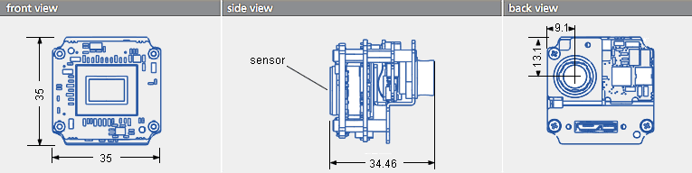
Standard model (BVS CA-SF1)
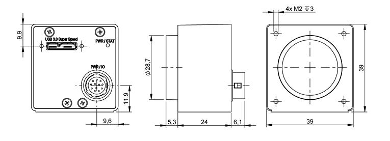
| BVS CA-SF1-xxxxxx-x6xx2x | |
| Size of body (w x h x l) | 39 x 39 x 24 mm |
| Lens protrusion | C-Mount | CS-Mount |
| 12.5 mm | 7.5 mm |
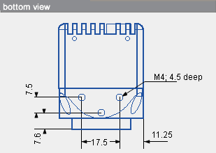
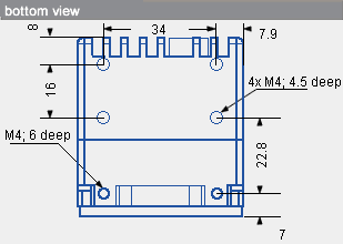
Mounting holes
On the bottom-side, the BVS CA-SF1 provides integrated tripod mounting holes.
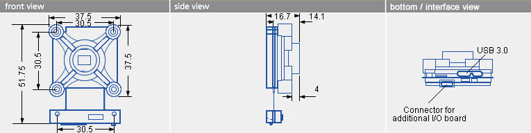
Standard model (BVS CA-SF2)
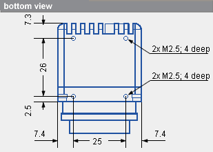
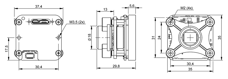
Option -11xxx (lensholder without back focus adjustment)
| BVS CA-SF2-xxxxxx-11xxxx | |
| Size of body (w x h x l) | 40 x 40 x 50.9 mm |
| Lens protrusion | |
| 10.7 mm with 1" lenses | |
Mounting holes
The BVS CA-SF2-xxxxxx-12xxxx provides integrated mounting holes.
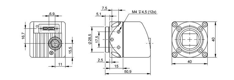
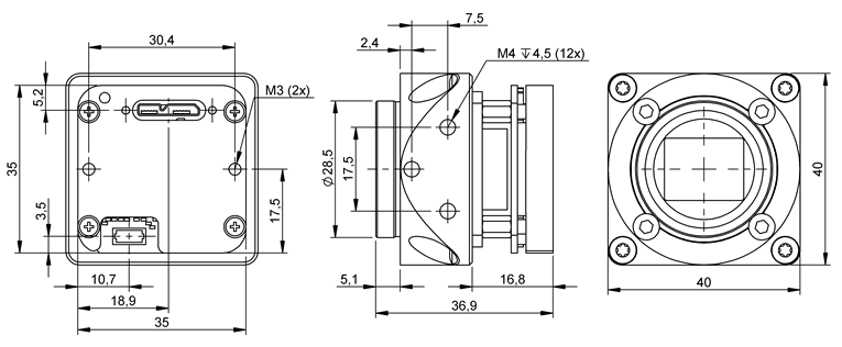
Option -12xxx (lensholder with back focus adjustment)
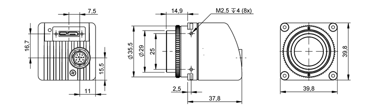
| BVS CA-SF2-xxxxxx-12xxxx | |
| Size of body (w x h x l) | 39.8 x 39.8 x 37.7 mm |
| Lens protrusion | C-Mount | CS-Mount |
| X | 8 mm | 6 mm |
| C-Mount | CS-Mount | |
| W | approx. 15 mm (C-mount) | approx. 10 mm (CS-mount) |
| Z | 17.526 mm (in air) | 12.5 mm (in air) |
Mounting holes
The BVS CA-SF2-xxxxxx-12xxxx provides integrated mounting holes.
Model without housing (BVS CA-SF1-xxxxxx-x00000)
- Attention
- "Broken connectors"
Handle the connectors with care otherwise you can damage the device.
→ In combination with the connectors, please limit the mechanical stress.
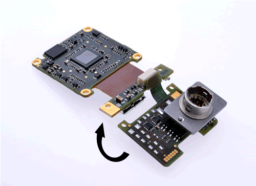
I/O board mvBlueFOX3-IO
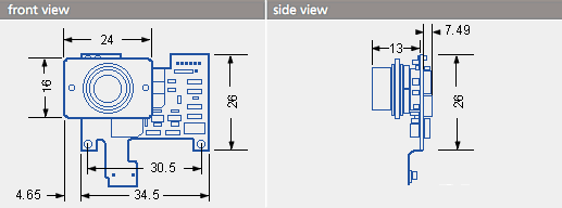
The following figure shows, how the additional I/O board mvBlueFOX3-IO gets connected correctly.
- Attention
- "Short circuit"
Since the connector of the I/O board will also fit upside down, you have to be careful while connecting. Otherwise you can destroy the camera and / or the I/O board.
→ As show in the figure, if the I/O board was connected correctly, you can bend the I/O board on the back of the sensor board. Then the I/O board connector will point to the opposite direction as the sensor.
The pinning of the mvBlueFOX3-IO is described in the chapter Circular connector male (Power / Digital I/O).
- Note
- There is also a version of the I/O board without connector as "mvBlueFOX3-IO NC" (NC = not connected). The pinning is provided in the figure:
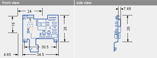
Figure 12: Dimensions of additional I/O board mvBlueFOX3-IO without connector
Model without housing (BVS CA-SF2-xxxxxx-xxx0xx)
- Attention
- "Broken connectors"
Handle the connectors with care otherwise you can damage the device.
→ In combination with the connectors, please limit the mechanical stress.
S-mount lensholder and heat sink backplate option (BVS CA-SF2-xxxxxx-xYx5xx)
The heat sink backplate is connected to the GND potential of the camera's power. The connection itself takes place via the fixing points. Both, the mounting holes on the lensholder (4x M2) as well as the mounting holes at the heat sink plate (2x M3) can be used to mount the camera.
- Attention
- "Overheating"
Wihtout a heat sink the device can be damaged.
→ Pay attention to the Overheating and Cooling .
C-mount lensholder and heat sink backplate option (BVS CA-SF2-xxxxxx-x1x51x)
The heat sink backplate is connected to the GND potential of the camera's power. The connection itself takes place via the fixing points. Both, the mounting holes on the lensholder (12x M4) as well as the mounting holes at the heat sink plate (2x M3) can be used to mount the camera.
- Attention
- "Overheating"
Wihtout a heat sink the device can be damaged.
→ Pay attention to the Overheating and Cooling .
| Lens protrusion | |
| X | 10.7 mm with 1" lenses |
| C-Mount | CS-Mount | |
| Z | 17.526 mm (in air) | 12.5 mm (in air) |
Fixed and compact C-mount lensholder (BVS CA-SF2-xxxxxx-x7x01x)
| Lens protrusion | |
| X | 13.1 +- 0.5 |
| C-Mount | |
| Z | 17.526 mm (in air) |
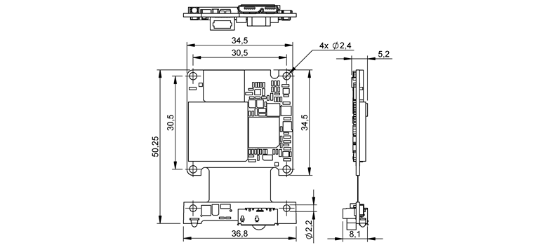
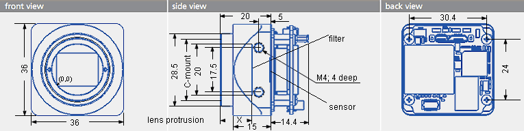
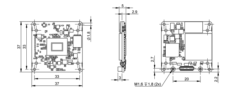
Single-board Model for Embedded Vision (BVS CA-SF3)
Hi-res model (BVS CA-SF4)
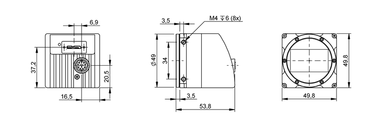
| BVS CA-SF4-xxxxxx-xNxx2x | |
| Size of body (w x h x l) | 49.8 x 49.8 x 54.215 mm |
Mounting holes
The BVS CA-SF4 provides integrated mounting holes.
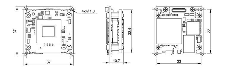
Board-level Model for Embedded Vision (BVS CA-SF5)
- Note
- The red dot marks pin 1.
Camera interfaces (BVS CA-SF)
Circular connector male (Power / Digital I/O)
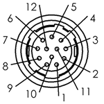
| Pin. | BVS CA-SF1 (Signal) | BVS CA-SF2 / BVS CA-SF4 (Signal) | Line in ImpactControlCenter | Cable KS-BCX-HR12 color scheme |
| 1 | GND (for PWR_IN) | black | ||
| 2 | not connected, leave open | PWR_IN | brown | |
| 3 | Opto DigOut3 | Line3 | red | |
| 4 | Opto DigIn0 | Line4 | orange | |
| 5 | Opto DigOut2 | Line2 | yellow | |
| 6 | Opto DigOut0 | Line0 | green | |
| 7 | Opto DigIn_GND | blue | ||
| 8 | RS232 RX | violet | ||
| 9 | RS232 TX | gray | ||
| 10 | Opto DigOut_PWR_IN | white | ||
| 11 | Opto DigIn1 | Line5 | white-black | |
| 12 | Opto DigOut1 | Line1 | white-brown | |
| Main connector shield | Main connector shield | Main shield | ||
Connector (camera side): SAMWOO SNH-10-12 (RPCB) or equivalent
Plug (matching cable plug): Hirose HR10A-10P-12S (01) or equivalent
Pinning of KS-BCX-HR12
| Pin. | CON 1 BVS CA-SF1 | Signal | CON 1 BVS CA-SF2 / BVS CA-SF4 | Signal | CON 2 open ended cable | Color |
| 1 | GND (for PWR_IN) | black | |
| 2 | not connected | PWR_IN | brown |
| 3 | DigOut3 (ImpactControlCenter numbering: line3) | red | |
| 4 | Opto DigIn0 (line4) | orange | |
| 5 | DigOut2 (line2) | yellow | |
| 6 | DigOut0 (line0) | green | |
| 7 | Opto DigIn GND | blue | |
| 8 | RS232_RX | violet | |
| 9 | RS232_TX | gray | |
| 10 | Opto DigOut_PWR_IN | white | |
| 11 | Opto DigIn1 (line5) | white-black | |
| 12 | Opto DigOut1 (line1) | white-brown | |
| Main connector shield | main shield | ||
Color assignment following international code for UL wiring.
Power Supply
The devcies are bus powered. Anyway, it is possible to power the BVS CA-SF2 externally with following specs:
- Input voltage range:
- 12 .. 24 V DC (typical)
- min. 10V
- max. 28V
- The power supply is protected against
- burst (EN 61000-4-4)
- surge (EN 61000-4-5) and
- polarity inversion
- internal short circuit protection by 1.5 A slow blow fuse
The USB power cannot be accessed via the I/O connector (this is prevented by a diode).
- Note
- The BVS CA-SF2 will reboot whenever you connect or disconnect the power at pin 2.
- Attention
- For BVS CA-SF4 an external power supply is obligatory (USB power supply may exceed 900 mA).
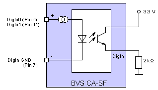
Characteristics of the digital inputs
Electrical characteristics
Delay
| Standard | |
| Notes | |
| High level | +3 to +24 V (max. 30 V) |
| Low level | 0 V (min. -30 V) to +0.7 V |
| Threshold (Low --> High / High --> Low) | 2 V +- 1 V |
| Imax | 5 mA |
|
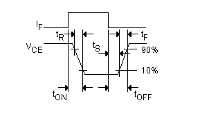
Switching characteristics
| Characteristics | Symbol | Test conditions | Typ. | Unit |
| Minimum trigger pulse width | 5 | us | ||
| Turn-On time | tON | R = 2 kOhm (Figure 7), internal output voltage 5 V, IF = 16 mA | 10 | |
| Storage time | tS | 25 | ||
| Turn-Off time | tOFF | 40 |
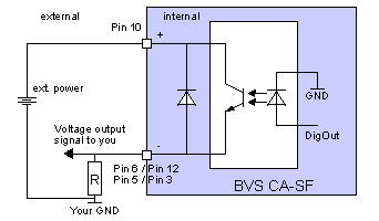
Characteristics of the digital outputs
Electrical characteristics
| Comment | Min. | Typ. | Max. | Unit | |
| IC | load current | 15 | mA | ||
| VCE(sat) | @ IC = 7 mA | 0.4 | V | ||
| VOUT | Output Voltage | 30 | V | ||
|
Switching characteristics
| Characteristics | Symbol | Test conditions | Typ. | Unit |
| Turn-On time | tON | RL = 100 Ohm, VCC 10 V, IC = 2 mA | 3 | us |
| Storage time | tS | 3 | ||
| Turn-Off time | tOFF | 3 | ||
| Turn-On time | tON | RL = 1.9 kOhm, VCC 5 V, IC = 16 mA | 10 | us |
| Storage time | tS | 25 | ||
| Turn-Off time | tOFF | 40 |
Status / Power LED
Standard model (BVS CA-SF1)
| State | LED color |
| No power, no USB connection or DeviceIndicatorMode is set to Inactive. | Off |
| No Bootloader found, Bootloader was recognized and FPGA is booting-up or device is in standby mode. | Red |
| mvBlueFOX3 is running. | Green |
| mvBlueFOX3 is busy (e.g. file upload). | Green blink |
Standard model (BVS CA-SF2)
| State | LED color |
| No power or DeviceIndicatorMode is set to Inactive. | Off |
| Bootloader was recognized and FPGA is booting-up. | White |
| mvBlueFOX3 is running. | Yellow |
| mvBlueFOX3 is streaming images. | Green |
| mvBlueFOX3 is busy (e.g. file upload). | Yellow blink |
| Waiting for USB connection with loaded FPGA (external power is connected). | White blink |
| Waiting for first USB connection, internal Error detected or device is put into standby. | Red |
| For HW Revision 2.01: Device is put into standby. | Turquoise |
BFembedded interface (BVS CA-SF3,BVS CA-SF5)
The BFembedded interface provides USB3.2 Gen.1 - SuperSpeed (5Gbps) including USB2.0 - Hi-Speed (480Mbps) and various IO functionality on a single 48-pin Board-to-Board connector. The main features of the user I/O interface are
- 4 digital inputs,
- 4 digital outputs,
- a UART interface for serial communication, and
- a I2C two wire serial interface.
- Attention
- "Disconnections"
When using BVS CA-SF3 or BVS CA-SF5 with the rigid-flex extension cable (BFE-FLEX), please ensure you have connected it correctly.
"Camera connector"
- Hirose DF40GB-48DP-0.4V
"Mating Connector"
Used for accessory IO Boards or customer implementation.
- Hirose DF40GB(3.0)-48DS-0.4V
"Mechanical characteristics"
- 48-pin, 0.4 mm pitch, shielded, stacking height: 3.0 mm
- 2 steel spacers (height 3mm). Thread M1.6, max. screw depth 1.8 mm.
Pin assignment
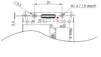
- Note
- The red dot marks pin 1 of Hirose DF40GB-48DP-0.4V.
| Pin | Signal | Description |
| 1 | VBUS_5V | USB Power |
| 2 | VBUS_5V | USB Power |
| 3 | VBUS_5V | USB Power |
| 4 | POWER_DOWN_N | - Complete power shut down
|
| 5 | VBUS_5V | USB Power |
| 6 | VAUX_PRESENT_N | - External power supply indication
|
| 7 | D- | USB 2.0 Data - (differential) |
| 8 | - | Do not connect, internal use |
| 9 | D+ | USB 2.0 Data + (differential) |
| 10 | - | Do not connect, internal use |
| 11 | ID | OTG-Identification (OTG = On-The-Go) |
| 12 | - | Do not connect, internal use |
| 13 | GND | Ground |
| 14 | - | Do not connect, internal use |
| 15 | GND | Ground |
| 16 | GND | Ground |
| 17 | GND | Ground |
| 18 | GND | Ground |
| 19 | SSTX- | USB3 Super Speed Transmitter (differential), polarity inversion allowed |
| 20 | - | Do not connect, internal use |
| 21 | SSTX+ | USB3 Super Speed Transmitter (differential), polarity inversion allowed |
| 22 | - | Do not connect, internal use |
| 23 | GND | Ground |
| 24 | - | Do not connect, internal use |
| 25 | SSRX+ | USB3 Super Speed Receiver (differential), polarity inversion allowed |
| 26 | - | Do not connect, internal use |
| 27 | SSRX- | USB3 Super Speed Receiver (differential), polarity inversion allowed |
| 28 | - | Do not connect, internal use |
| 29 | GND | Ground |
| 30 | - | Do not connect, internal use |
| 31 | GND | Ground |
| 32 | GND | Ground |
| 33 | GND | Ground |
| 34 | GND | Ground |
| 35 | DigOut0 | Digital Output (with level shifter), voltage reference VCC_IO |
| 36 | VCC_IO | I/O voltage reference input 1.8 V...5.0 V, abs. min max: 1.65 V...5.5 V
|
| 37 | DigOut1 | Digital Output (with level shifter), voltage reference VCC_IO |
| 38 | DigIn2 | Digital Input (with level shifter), voltage reference VCC_IO |
| 39 | DigOut2 | Digital Output (with level shifter), voltage reference VCC_IO |
| 40 | DigIn3 | Digital Input (with level shifter), voltage reference VCC_IO |
| 41 | DigOut3 | Digital Output (with level shifter), voltage reference VCC_IO |
| 42 | UART_RX | Serial interface (see details below), LVCMOS 3.3 V IO level |
| 43 | DigIn0 | Digital Input (with level shifter), voltage reference VCC_IO |
| 44 | UART_TX | Serial interface (see details below), LVCMOS 3.3 V IO level |
| 45 | DigIn1 | Digital Input (with level shifter), voltage reference VCC_IO |
| 46 | I2C_SCL | I2C two wire serial bus (see details below), LVCMOS 3.3 V IO level |
| 47 | - | Do not connect, internal use |
| 48 | I2C_SDA | I2C two wire serial bus (see details below), LVCMOS 3.3 V IO level |
- Note
- Additional shield pins are connected to GND.
Electrical characteristics of signals
USB Power
| Signal | Parameter | min | nom | max | Unit |
| VBUS_5V | 4.45 | 5 | 5.25 | V | |
| IVBUS_5V* | 900 | mA | |||
| I per pin | 300 | mA |
*Limit for USB3 high-power SuperSpeed devices (Power consumption of the camera will be within this limit).
The rated current limit for the connector is 300 mA per pin and therefore the BF3-Embedded Interface would allow up to 1200 mA.
VCC_IO / DIGIN / DIGOUT
| Signal | Parameter | min | nom | max | Unit |
| VCC_IO | I/O voltage power | 1.65 | 5.5 | V | |
| UDIG_IN_LOW | VIL (low level input voltage) | VCC_IO x 0.3 | V | ||
| UDIG_IN_HIGH | VIH (high level input voltage) | VCC_IO x 0.7 | V | ||
| IOH | High-level output current VCC_IO: 4.5 V to 5.5 V | -32 | mA | ||
| IOL | Low-level output current VCC_IO: 4.5 V to 5.5 V | 32 | mA | ||
| UDIG_OUT_HIGH | Digital output (VCC_IO = 4.5 V / IOUT= -32 mA) | 3.8 | V | ||
| UDIG_OUT_LOW | Digital output (VCC_IO = 4.5 V / IOUT= 32 mA) | 0.55 | V |
Digital I/Os include level shifters to allow customized IO Levels for both inputs and outputs. VCC_IO (Pin 36) is the input for the user defined IO voltage.
- Note
- If no I/O functionality is needed, connect VCC_IO to VBUS_5V.
For other output characteristics, see datasheet SN74LVC2T45.
Serial Interface, I2C and Power Down
| Signal | Parameters / Properties | min | nom | max | Unit |
| POWER_DOWN_N | Complete power shut down, internal 10K pull up to VBUS_5V | ||||
| POWER_DOWN_N Input Low Voltage | 0 | 0.75 | V | ||
| POWER_DOWN_N Input High Voltage | 1.8 | 5 | V | ||
| UART_RX / UART_TX | Voltage level
| 3.3 | 3.4 | V | |
| I2C_SCL / I2C_SDA | Voltage level, internal 2K pull up to 3.3 V
| 3.3 | 3.4 | V |
Boards for the BFembedded interface (BVS CA-SF3,BVS CA-SF5)
USB Micro B (horizontal)
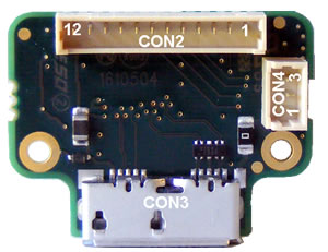
The board includes a USB3 Micro B connector (CON3) in horizontal alignment, a 12-pin header (CON2) for IO signals and a 3-pin header (CON4) for I2C, weight 2g.
"Order Code": BFE-IF-MICUSB3B-H-IO12
USB Micro B (vertical)
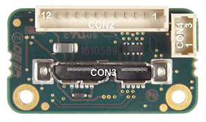
The board includes a USB3 Micro B connector (CON3) in vertical alignment, a 12-pin header (CON2) for IO signals and a 3-pin header (CON4) for I2C, weight 2g.
"Order Code": BFE-IF-MICUSB3B-V-IO12
USB Type C
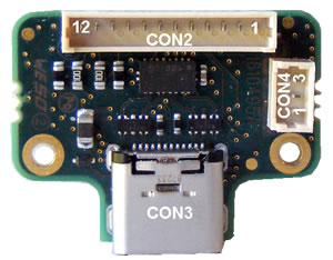
The board includes a USB Type C connector (CON3) in horizontal alignment, a 12-pin header (CON2) for IO signals and a 3-pin header (CON4) for I2C, weight 2g.
"Order Code": BFE-IF-USB3C-H-IO12
Pin assignments
12-pin I/O connector (CON2)
- Part type:
- Wire-to-Bord Connector 1.25 mm, WUERTH_653012114822 or MOLEX PicoBlade 53047_1210
- Connecting part:
- Würth: 653 012 113 322 1.25 MM female terminal housing with female crimp terminal WR-WTB 653 001 137 22 or
- Molex 0510211200, 1.25 Wire to Board Connection Receptacle Housing, Applicable Terminal 50058-8000, 50079-8000 Series
| Pin | I/O | Signal | Description |
| 1 | Out | DigOut0 | Digital Output |
| 2 | Out | DigOut1 | Digital Output |
| 3 | Out | DigOut2 | Digital Output |
| 4 | Out | DigOut3 | Digital Output |
| 5 | In | DigIn0 | Digital Input |
| 6 | In | DigIn1 | Digital Input |
| 7 | In | DigIn2 | Digital Input |
| 8 | In | DigIn3 | Digital Input |
| 9 | Out | RS232_TXD | Serial Interface RS232_TXD |
| 10 | In | RS232_RXD | Serial Interface RS232_RXD |
| 11 | GND | GND | Ground |
| 12 | POWER_OUT | VBUS_OUT | Directly connected to USB Power |
"Electrical characteristics of signals"
"VBUS_OUT / DIGIN / DIGOUT"
| Signal | Parameter | min | nom | max | Unit |
| VBUS_OUT | 4.45 | 5.00 | 5.25 | V | |
| IVBUS_OUT | 10 | mA | |||
| UDIG_IN_LOW | VIL (low level inputvoltage) | 0.3 | V | ||
| UDIG_IN_HIGH | VIH (high level inputvoltage) | 0.7 | 5.5 | V | |
| IOH | High-level output current | -32 | mA | ||
| IOL | Low-level output current | 32 | mA | ||
| UDIG_OUT_HIGH | Digital output (IOUT= -32 mA) | 3.8 | V | ||
| UDIG_OUT_LOW | Digital output (IOUT= 32 mA) | 0.45 | V |
"Serial interface RS232"
| Signal | Test Properties | min | nom | max | Unit |
| EIA/TIA-232E Input Voltage Range* | -30 | +30 | V | ||
| EIA/TIA-232E Input Threshold Low | 0.6 | 1.3 | V | ||
| EIA/TIA-232E Input Threshold High | 1.6 | 2.4 | V | ||
| EIA/TIA-232E Input Hysteresis | 0.4 | mA | |||
| EIA/TIA-232E Input Resistance | 3 | 5 | 7 | V | |
| Output Voltage Swing | ±5.0 | ±5.7 | V | ||
| RS-232 Output Short-Circuit Current | ±15 | mA | |||
| ESD PROTECTION | Human body model air discharge Human body model contact discharge | ±15 ±8 | kV kV | ||
| TIMING CHARACTERISTICS Maximum Data Rate | 460 | kbps |
* Guaranteed by design.
USB Micro B Connector (CON3)
- Standard USB3.0 Micro-B Connector
- Part Type: WUERTH_ 692 622 030 100
| Pin | I/O | Signal | Description |
| 1 | Power_IN | VBUS_IN | Digital Output |
| 2 | In/Out | D- | USB 2.0 Data −(differential) |
| 3 | In/Out | D+ | USB 2.0 Data +(differential) |
| 4 | IN | ID | OTG-Identification (OTG= On-The-Go) |
| 5 | GND | GND | Ground to Pin 1 |
| 6 | In/Out | SSTX- | Super Speed Transmitter(differential) |
| 7 | In/Out | SSTX+ | Super Speed Transmitter(differential) |
| 8 | GND | GND | Ground for Super SpeedSignale |
| 9 | In/Out | SSRX+ | Super Speed Receiver(differential) |
| 10 | In/Out | SSRX- | Super Speed Receiver (differential) |
| Shell | Shield | Shield |
"Electrical characteristics of signals"
| Signal | Parameter | min | nom | max | Unit |
| VBUS_IN | 4.45 | 5.00 | 5.25 | V | |
| IVBUS_IN | 900 | mA |
USB Type C Connector (CON3)
- Standard USB3.2 Gen.1 TYPE-C, Connector Type: JAE_DX07S024JJ2
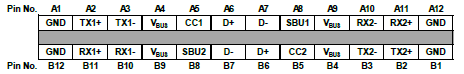
| Pin | I/O | Signal | Description |
| A1 | GND | GND | Ground for Super Speed Signals |
| A2 | In/Out | SSTX1+ | Super Speed Transmitter (differential) |
| A3 | In/Out | SSTX1- | Super Speed Transmitter (differential) |
| A4 | Power_IN | VBUS_IN | Digital Output |
| A5 | IN | CC1 | Configuration Channel |
| A6 | In/Out | D+ | USB 2.0 Data + (differential) |
| A7 | In/Out | D- | USB 2.0 Data - (differential) |
| A8 | – | NC | Sideband Use → Alternate Mode |
| A9 | Power_IN | VBUS_IN | Digital Output |
| A10 | In/Out | SSRX2- | Super Speed Receiver (differential) |
| A11 | In/Out | SSRX2+ | Super Speed Receiver (differential) |
| A12 | GND | GND | Ground for Super Speed Signals |
| B1 | GND | GND | Ground for Super Speed Signals |
| B2 | In/Out | SSTX1+ | Super Speed Transmitter (differential) |
| B3 | In/Out | SSTX1- | Super Speed Transmitter (differential) |
| B4 | Power_IN | VBUS_IN | Digital Output |
| B5 | IN | CC1 | Configuration Channel |
| B6 | In/Out | D+ | USB 2.0 Data + (differential) |
| B7 | In/Out | D- | USB 2.0 Data - (differential) |
| B8 | – | NC | Sideband Use > Alternate Mode |
| B9 | Power_IN | VBUS_IN | Digital Output |
| B10 | In/Out | SSRX1- | Super Speed Receiver (differential) |
| B11 | In/Out | SSRX1+ | Super Speed Receiver (differential) |
| B12 | GND | GND | Ground for Super Speed Signals |
| Shell | Shield | GND | Shield |
"Electrical characteristics of signals"
| Signal | Parameter | min | nom | max | Unit |
| VBUS_IN | 4.45 | 5.00 | 5.25 | V | |
| IVBUS_IN | 900 | mA |
3-pin I2C connector (CON4)
- Part type:
- Wire to Bord Connector 1.25 mm, WUERTH_653003114822 or MOLEX PicoBlade 53047_0310
- Mating part:
- Würth: 653 003 113 322 1.25 MM female terminal housing with female crimp terminal WR-WTB 653 001 137 22 or
- Molex 0510210300, 1.25 Wire to Board Connection Receptacle Housing, Applicable Terminal 50058-8000, 50079-8000 Series
| Pin | I/O | Signal | Description |
| 1 | - | GND | Camera GND |
| 2 | Out | SCL | I2C Clock |
| 3 | Bi | SDA | I2C data |
"Electrical characteristics of signals"
- Camera provides a I2C master to control devices connected to the bus
- Interface clock rate 400kHz
- Reserved I2C addresses (8Bit) of shared devices: 0x0, 0x30...0x36, 0x48, 0x60...0x66, 0xA0...0xA6, 0xB0...0xBE, 0xF8
- Access to the I2C interface has to be enabled
- By default the access to the I2C bus is disabled to prevent unintended interference
- See also
- API documentation: https://assets.balluff.com/documents/DRF_957355_AA_000/classmv_1_1impact_1_1acquire_1_1GenICam_1_1mvI2cInterfaceControl.html
| Signal | Parameters / Properties | min | nom | max | Unit |
| I2C_SCL / I2C_SDA | Voltage level, internal 2K pull up to 3.3 V | 3.3 | 3.4 | V |
Components
1 for board level cameras follow cooling recommendations in "BVS CA-SF3 / BVS CA-SF5: Cooling instructions" and "BVS CA-SF2: Cooling
instructions" which are part of the scope of delivery
2 not evaluated by UL