Loading...
Searching...
No Matches
Technical Data
Power supply
| Symbol | Comment | Min | Typ | Max | Unit |
| UUSBPOWER_IN | Power supply via USB | 4.75 | 5 | 5.25 | V |
| IUSBPOWER_IN (@ 5V / 40MHz) | 280 | 500 | mA | ||
| IUSBPOWER_IN (Power Off Mode) | 66 | mA |
Single-board version (BVS CA-MLC)
Typical Power consumption @ 5V
| Model | Power consumption (+/- 10%) | Unit |
| -200w | 1.09 | W |
| -202a | 1.39 | W |
| -202b | 1.58 | W |
| -202d | 1.28 | W |
| -202v | 1.35 | W |
| -205 | 1.37 | W |
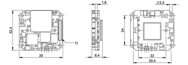
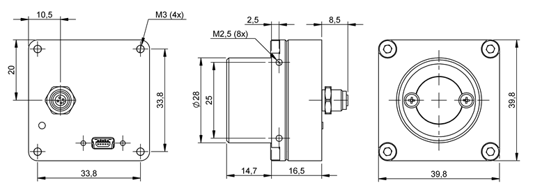
Dimensions and connectors
- Note
- The BVS CA-MLC has a serial I²C bus EEPROM with 16 KByte of which 8 KByte are reserved for the firmware and 8 KByte can be used to store custom arbitrary data.
- See also
- UserDataEntry class description
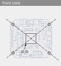
Sensor's optical midpoint and orientation
The sensor's optical midpoint is in the center of the board (Figure 2: intersection point of the holes diagonals). The (0,0) coordinate of the sensor is located at the one bottom left corner of the sensor (please notice that Mini-B USB connector is located at the bottom at the back).
- Note
- Using a lens, the (0,0) coordinate will be mirrored and will be shown at the top left corner of the screen as usual!
Mini-B USB (USB 2.0)

| Pin | Signal | Comment |
| 1 | USBPOWER_IN | Supply voltage |
| 2 | USB_DATA- | Data |
| 3 | USB_DATA+ | Data |
| 4 | ID | Not connected |
| 5 | GND | Ground |
12-pin Wire-to-Board header (USB 2.0 / Dig I/O)
- Note
- If you have the BVS CA-MLC variant which uses the standard Mini-B USB connector, pin 2 and 3 (USB_DATA+ / USB_DATA-) of the header won't be connected!
| pin | Opto-isolated variant | TTL compliant variant | Cable KS-MLC-USB2-IO-W | Cable KS-MLC-IO-W | ||
| Signal | Comment | Signal | Comment | |||
| 1 | GND | Ground | GND | Ground | GND | |
| 2 | USB_DATA+ | Data | USB_DATA+ | Data | USB_DATA+ | |
| 3 | USB_DATA- | Data | USB_DATA- | Data | USB_DATA- | |
| 4 | USBPOWER_IN | Supply voltage | USBPOWER_IN | Supply voltage | USBPOWER_IN | |
| 5 | I2C SDA | Serial data line (the I2C interface is master-only, which means that I2C slaves can only be connected externally) | I2C SDA | Serial data line | ||
| 6 | I2C SCL | Serial clock line (the I2C interface is master-only, which means that I2C slaves can only be connected externally) | I2C SCL | Serial clock line | ||
| 7 | USBPOWER_IN | Supply voltage | USBPOWER_IN | Supply voltage | red | |
| 8 | GND | Ground | GND | Ground | black | black |
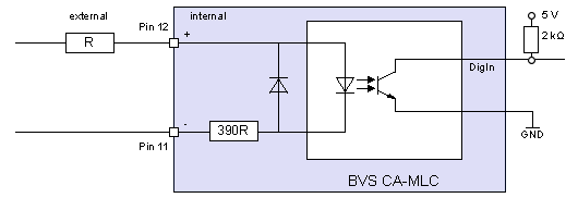
| 9 | OUT0- | Opto-isolated digital output 0 (Negative voltage) | OUT1 | TTL compliant digital output 1 | blue | blue |
| 10 | OUT0+ | Opto-isolated digital output 0 (Positive voltage) | OUT0 | TTL compliant digital output 0 | violet | violet |
| 11 | IN0- | Opto-isolated digital input 0 (Negative voltage) | IN1 | TTL compliant digital input 1 | gray | gray |
| 12 | IN0+ | Opto-isolated digital input 0 (Positive voltage) | IN0 | TTL compliant digital input 0 | pink | pink |
- Note
- I2C bus uses 3.3 Volts. Signals have a 2kOhm pull-up resistor. Access to the I2C bus from an application is possible for BVS CA-MLC devices using Impact Acquire with version 1.12.44 or newer.
Manufacturer (suitable board-to-wire connector): Molex
Part number: 0510211200 1.25mm Housing
Link: https://www.molex.com/en-us/products/part-detail/510211200
Manufacturer (multi-pin connector for board-to-board connection): e.g. Garry
Link: http://www.mpe-connector.de/index.php?lang=de&menu=16&mating=1841&id_product=6591 (recommended variant: 659-1-012-O-F-RS0-xxxx; xxxx = length of the pins)
- See also
- Suitable assembled cable accessories for BVS CA-MLC: What's inside and accessories
- High-Speed USB design guidelines
- More information about the usage of retrofittable ferrite
Electrical characteristic
Digital inputs TTL
- Note
- If the digital input is not connected, the state of the input will be "1" (as you can see in ImpactControlCenter).
| TTL compliant variant | |||||
| Comment | Min | Typ | Max | Unit | |
| IIN | ILOW (INx) | -0.5 | mA | ||
| UIN | VIH | 3.6 | 5.5 | V | |
| VIL | -0.3 | 1.3 | V | ||
| LVTTL compliant variant | |||||
| Comment | Min | Typ | Max | Unit | |
| IIN | ILOW (INx) | -0.5 | mA | ||
| UIN | VIH | 2 | 3.8 | V | |
| VIL | -0.3 | 0.8 | V | ||
TTL input low level / high level time: Typ. < 210ns
Digital outputs TTL
| Comment | Min | Typ | Max | Unit | |
| IOUT | Dig_out power | +-32 | mA | ||
| UOUT | VOH (IOUT=32mA) | 3.8 | V | ||
| VOH | 5.25 | ||||
| VOL (IOUT=32mA) | 0.55 | V | |||
| VOL | 0.1 |
TTL output low level / high level time: Typ. < 40ns
Opto-isolated digital inputs
Delay
| Characteristics | Symbol | Typ. | Unit |
| Turn-On time | tON | 3 | us |
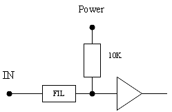
The inputs can be connected directly to +3.3 V and 5 V systems. If a higher voltage is used, an external resistor must be placed in series (Figure 6).
| Used input voltage | External series resistor |
| 3.3V .. 5V | none |
| 12V | 680 Ohm |
| 24V | 2 KOhm |
| Comment | Min | Typ | Max | Unit | |
| UIN | VIH | 3 | 5.5 | V | |
| VIL | -5.5 | 0.8 | V |
Opto-isolated digital outputs
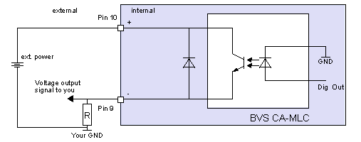
Delay
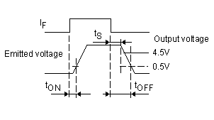
| Characteristics | Symbol | Test conditions | Typ. | Unit |
| Turn-On time | tON | RL = 1.9 kOhm, VCC 5V, IC = 16mA | 2 | us |
| Storage time | tS | 25 | ||
| Turn-Off time | tOFF | 40 |
| Comment | Min | Typ | Max | Unit | |
| Ion | load current | 15 | mA | ||
| Ioff | leakage current | 10 | uA | ||
| Von Sat. at 2.4 mA | VIH | 0 | (0.2) | 0.4 | V |
| Voff | 30 | V |
LED states
| State | LED |
| Camera is not connected or defect | LED off |
| Camera is connected but not initialized or in "Power off" mode. | Orange light on |
| Camera is connected and active | Green light on |
Assembly variants
The BVS CA-MLC is available with following differences:
- Mini-B USB connector and digital I/O pin header
- 1/1 opto-isolated or 2/2 TTL compliant digital I/O
- USB via header without Mini-B USB connector
- female board connector instead of pin header (board-to-board connection)
- 3 different S-mount depths
- C(S)-mount compatibility using mvBlueCOUGAR-X flange
- ambient temperature operation: 5..55 deg C / 30..80 RH
- ambient temperature storage: -25..60 deg C / 20..90 RH
Single-board version with housing (BVS CA-IGC)
Dimensions and connectors
| Lens protrusion | C-Mount | CS-Mount |
| X | 10 mm | 5 mm |
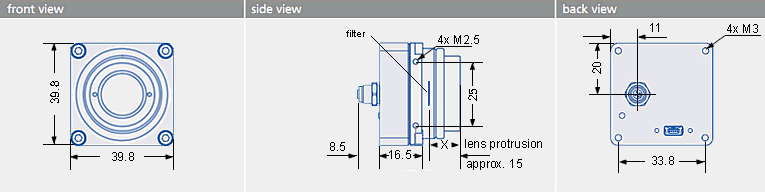
| Lens protrusion | C-Mount |
| X | 8 mm (9.5 mm with max. Ø 20 mm) |
- Note
- The BVS CA-IGC has a serial I²C bus EEPROM with 16 KByte of which 8 KByte are reserved for the firmware and 8 KByte can be used to store custom arbitrary data.
- See also
- UserDataEntry class description
Mini-B USB (USB 2.0)
| Pin | Signal | Comment |
| 1 | USBPOWER_IN | Supply voltage |
| 2 | USB_DATA- | Data |
| 3 | USB_DATA+ | Data |
| 4 | ID | Not connected |
| 5 | GND | Ground |
4-pin circular plug-in connector with lock (I/O)
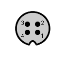
| Pin | Signal | Comment | Color (of cable) |
| 1 | IN0 + | Opto-isolated digital input 0 (Positive voltage) | brown |
| 2 | IN0 - | Opto-isolated digital input 0 (Negative voltage) | white |
| 3 | OUT0 + | Opto-isolated digital output 0 (Positive voltage) | blue |
| 4 | OUT0 - | Opto-isolated digital output 0 (Negative voltage) | black |
Manufacturer: Binder
Part number: 79-3107-52-04
Electrical characteristic
Please have a look at the BVS CA-MLC digital I/O characteristics (opto-isolated model) of the 12-pin Wire-to-Board Header (USB / Dig I/O).
LED states
| State | LED |
| Camera is not connected or defect | LED off |
| Camera is connected but not initialized or in "Power off" mode. | Orange light on |
| Camera is connected and active | Green light on |
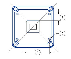
Positioning tolerances of sensor chip
The sensor's optical midpoint is in the center of the housing. However, several positioning tolerances in relation to the housing are possible because of:
- Tolerance of mounting holes of the printed circuit board in relation to the edge of the lens holder housing is not specified but produced according to general tolerance DIN ISO 2768 T1 fine.
- Tolerance of mounting holes on the printed circuit board because of the excess of the holes ± 0.1 mm (Figure 13; 2).
- Tolerance between conductive pattern and mounting holes on the printed circuit board.
Because there is no defined tolerance between conductive pattern and mounting holes, the general defined tolerance of ± 0.1 mm is valid (Figure 13; 1 in the Y-direction ± 0.1 mm; 3 in the Z-direction ± 0.1 mm)
There are further sensor specific tolerances, e.g. for model BVS CA-MLC-0004ZG:
- Tolerance between sensor chip MT9V034 (die) and its package (connection pad)
- Chip position in relation to the mechanical center of the package: 0.2 mm (± 0.1mm) in the X- and Y-direction (dimensions in the sensor data sheet according to ISO 1101)
- Tolerance between copper width of the sensor package and the pad width of the printed circuit board
During the soldering the sensor can swim to the edge of the pad: width of the pad 0.4 mm (possible tolerance is not considered), width of pin at least 0.35 mm, max. offset: ± 0,025mm
Further specific tolerances of other models on request.
- Note
- There are also tolerances in lens which could lead to optical offsets.
Summary of components
| Features | -MLC | -IGC | |||
| "-xOx-" | "-xTx-" | "-xLx-" | -xxx2 | ||
| Image Memory | 8 Mpixels | ||||
| ADC resolution | CMOS: 10 bits (10/8 bit transfer) | ||||
| Inputs | 1 | 2 | 3 | 1 | |
| Type | opto-isolated | TTL | LVTTL | opto-isolated | |
| Outputs | 1 | 2 | x | 2 | |
| Type | opto-isolated | TTL | x | opto-isolated | |
| USB 2.0 | Mini-B USB (-xxW-) / 12-pin Wire-to-Board header (-xxB-) / Mini-B USB (-xxA-) | Mini-B USB | |||
| Optics | |||||
| Lens Mount (Focal Distance) | C-mount (17.526 mm in air), CS-mount (12.5 mm in air), optional S-mount | C-mount (17.526 mm in air), CS-mount (12.5 mm in air) | |||
| Environment | |||||
| Ambient Temperature | |||||
| Operation | 0..45 deg C / 30 to 80% RH | ||||
| Storage | -20..60 deg C / 20 to 90% RH | ||||
| Protection class 1 | IP40 | ||||
| Weight without lens | approx. 10 g | approx. 80 g | |||
| Power supply (PWR_IN) | |||||
| DC | 4.75 to 5.25 V via USB | ||||
| Pmax | 1.5 W | ||||
| Peak current draw | 0.5 A | ||||
1 not evaluated by UL
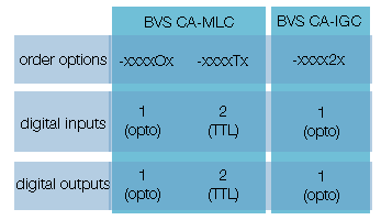
Summary of available digital I/O's